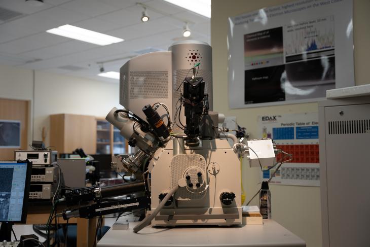
This is a "dual beam" scanning electron microscope (SEM) that is also equipped with a focused ion beam (FIB). This SEM functions permit microscopic observations of a specimen while the FIB functions allows cutting of your sample. This FEG-SEM-FIB has an Omniprobe for TEM sample preparation. A 30 mm^2 new (2019) Noran SDD EDS with Compass (principal components analysis for phase ID) analyzes specimen elemental chemistry.
In addition, an EDAX "digi view" electron backscattered diffraction system (EBSD) collects the crystallography information from the specimen. The Quanta 3D, also has the fast beam blanker and Nanometer Pattern Generation System for E and I beam lithography.
With prototypical photo resists from the Keszler lab we have achieved 8 nm line widths on isolated lines. Using PMMA we routinely obtain 20 nm line widths on periodic structures. While the Quanta 3D does have auto slice n view and STEM, much better versions of those are available on our Helios.
Features
- Field emission electron source with probe current continuously adjustable up to 200 nA
- Beam acceleration voltages selectable from 200 volts to 30 kilovolts
- Spatial resolution 1.2 nm in secondary electron imaging mode, 0.8 nm in STEM imaging mode
Magnification range from 30x to 1,280kx. Although, it lacks a through the lens detector and so practical magnification is limited to around 100,000x. - Motorized 5 axis specimen stage
- Focused ion beam (FIB) allows specimens to be eroded and modified during viewing
- Specimen etch or deposition (currently with C and Pt) capability, selection of up to 5 gas injectors possible
- X-Ray Energy Dispersive Spectrometer (EDS) provides elemental composition spectra acquisition, elemental distribution mapping, and line transect element profiling capabilities
- Electron Backscattered Diffraction (EBSD) or Orientation Imaging Microscopy (OIM) allows crystal structure information to be collected
- Variable pressure vacuum system with high vacuum, low vacuum obtainable only after inserting a special plug in the pole piece.
- Scanning transmission electron detector (STEM)
- Nanopattern Generation System (NPGS) or E-Beam & Ion-Beam Lithography allows nano-devices to be fabricated on substrates