Image
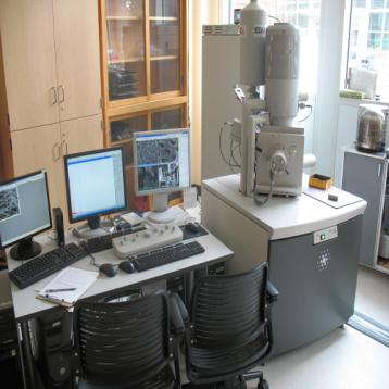
The Nova SEM field emission scope has an imersion lens or through the lens detector for high resoution imaging. Like our other tools it also has an X-ray detector for EDS semi quant work. The tool is especially suited for nano-materials applications.
Features
This is a high resolution tool with a through the lens detector. It really comes into play above 100,000x magnification.
- Field emission electron source, with probe current to 10 nA (high resolution mode), 22 nA (analytical mode)
- Beam acceleration voltages selectable from 200 volts to 30 kilovolts
- Beam deceleration option minimizes beam damage to sensitive specimens, beam impact energy as low as 50 volts
Six electron image signal detectors:
- In-lens secondary electron detector [a.k.a. "immersion" or "through-the-lens" (TLD) secondary electron (SE) detector, TLD-SE]
- In-lens BSE detector (through-the-lens detector, backscatterd electron, TLD-BSE)
- Everhart-Thornley detector (ETD) [conventional "below-the-lens" detector]
- Solid state scanning transmitted electron (STEM) detector
- Gaseous analytical detector (GAD) low kV backscattered electron detector is availabe but not in use yet.
- Low vacuum secondary electron detector (LVD) for use with non-conductive samples
Resolution at optimum working distance:
- 1.0 nm at 15 kV (TLD-SE)
- 1.6 nm at 1 kV (TLD-SE)
- 0.8 nm at 30 kV (STEM)
Motorized 4 axis stage assures precise, reproducible specimen positioning.
X-Ray Energy Dispersive Spectrometer (EDS) for elemental spectra, mapping.