EDS linescan of Alumina layer on metal
EDS linescan of Alumina layer on metal
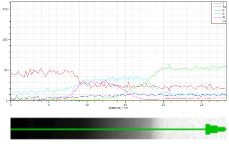
STEM EDS profile through a Thin film device, tunnel diode, made here at OSU. By doing long count maps we can post process the hypermap into line scans in any direction you want!
Image